We stand at the tipping point of a new technological generation, marked by the rise of AI. As data-intensive applications vie for greater computational capabilities and faster transfer speeds, flash memory innovation must continue to accelerate to keep pace with the surge in compute demand and mitigate the accompanying challenge of crippling power consumption in data centers. Higher densities and more energy efficiencies in 3D NAND chips will be essential to not only address performance, space and power requirements, but to keep operating costs manageable while counteracting the potential environmental impact of the AI era.
Some memory manufacturers have predicted scaling 3D NAND to 1,000 layers within this decade, but the technologies and processes that got us from 2D to 3D, and from 64- to 232-layer 3D NAND are not capable of achieving such unprecedented scale. It will require Lam’s coolest technological breakthrough yet—pushing physics and chemistry to their limits, striving for higher storage capacities and data processing speeds never achieved before in solid-state drives (SSDs).
Building on two decades of leading-edge innovations in dielectric etch technology, Lam Research introduced Lam Cryo™ 3.0 to help overcome the most critical challenges in scaling production of AI-ready 3D NAND.
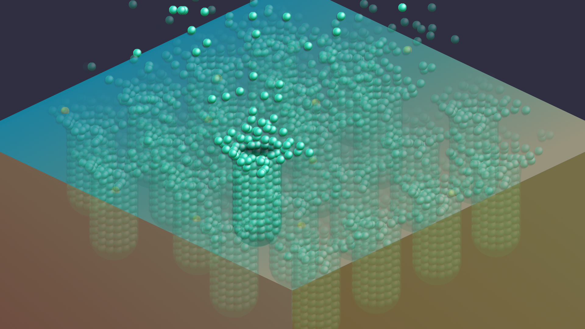
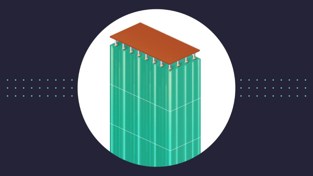
3D NAND flash involves stacking multiple layers of cells to achieve higher densities for increased data storage capacity and throughput—crucial for AI, Machine Learning and applications that require rapid data retrieval and processing. Creating such architectures involves almost unfathomable complexity for manufacturing at the atomic scale—1,000x smaller than the width of a human hair.
Etching material from the surface of a wafer to achieve desired patterns and memory cell structures is a critical process to enhance 3D NAND device performance, reliability and yield. So, the question of how to achieve higher aspect ratio (HAR) etching—at ever-greater depths and with more precision without compromising quality—has been a hot topic in the semiconductor industry for years.
For Lam, it was about cooling things down. Way down!
Delivering angstrom-level control of lateral and vertical feature profiles, Lam Cryo 3.0 leverages subzero processing temperatures to enable novel chemistries for etching memory channels of up to 10 microns in depth without compromising critical shape dimensions.
When it comes to etching, “memory channel precision” refers to creating vertical pathways in the memory stack that connect the cells, which is vital for scaling 3D NAND devices to higher layer counts. “Logic scaling” requires maintaining top-to-bottom dimensionality of the channels, which is essential for enabling each memory cell to store more bits and increase the performance and capacity of flash memory as it scales to more layers and taller stacks. And beyond this technical complexity for increasing performance and capacity, flash manufacturers must also decrease the operational costs per bit to achieve scale.
Lam’s pioneering efforts in etch and deposition technology over the decades have led to many significant breakthroughs in NAND flash manufacturing using our unique and proprietary technologies, including cryogenic memory channel etch. By lowering wafer temperatures during manufacturing, Lam can leverage novel process chemistries to enable more bits per cell for scaling devices to higher layer counts with deeper etches and greater uniformity than ever before.
Lam Cryo 3.0 represents a significant leap forward in cryogenic etching technology to transform 3D NAND chip manufacturing as it works to meet the demands of the AI era.
Lam played a leading role in the industry’s transition from planar to 3D NAND with its HAR etch solutions that deliver top-to-bottom feature precision. Since 2019, Lam has been the only company with production-proven cryogenic tools for manufacturing advanced NAND devices, boasting a worldwide customer install base of nearly 1,000 chambers used to process over five million wafers.
“Lam Cryo 3.0 cryogenic etch technology is a significant leap beyond conventional techniques,”
says Neil Shah, co-founder and vice president of research at Counterpoint Research.
“It etches memory channels that are more than 50 times deeper than their width with near perfect precision and control, achieving a profile deviation of less than 0.1%. This breakthrough significantly enhances advanced 3D NAND yields and overall performance, enabling chipmakers well in the AI era.”
Lam’s cryogenic etch technology combines industry-leading high-power confined plasma reactors and pulsed plasma reactor technology with processing temperatures that can reach well below 0oC. This enables new chemistries for HAR etches essential in scaling 3D NAND layer counts.
With these cryogenic etch innovations, Lam is enabling today’s leading flash memory manufacturers to achieve near-perfect etching profiles for higher throughput, greater efficiencies, and lower environmental impact needed to support next-generation applications. What’s more, manufacturers can scale 3D NAND laterally, vertically, and logically – increasing bit density and capacity from single-level cell (SLC) up to quad-level cell (QLC) for higher storage capacity, performance and energy efficiency.
What’s Cool about Lam Cryo?
With etch rates more than twice as fast as conventional dielectric etching, Lam’s cryogenic etch technologies enable cost-effective bit scaling for faster production and higher yield, with unmatched precision to repeatedly etch memory channels as deep as 10 microns with less than 0.1% deviation* of critical top-to-bottom dimensions. Not only can customers leverage Lam’s cryo-enabled tools while continuing to utilize previously installed etch systems, but the technologies also have the potential to reduce carbon footprints by using novel process gases (and their byproducts) that have a lower overall environmental impact. Furthermore, higher throughput results in lower overall system energy usage with an anticipated 40% reduction in energy consumption per wafer** and a 90% reduction in emissions***.
As we enter the AI age, reaching 1,000-layer 3D NAND represents more than just a technological aspiration; it symbolizes a new paradigm for the semiconductor industry as we work to meet the intensive data processing and storage demands of today and beyond. Lam Research is committed to leading this charge, providing cryogenic solutions and other innovations to help overcome the most critical technological, economic, and manufacturing operational challenges to usher in the AI era.
Tae Won Kim is CVP of Global Products – Dielectric Etch at Lam Research
* Profile deviation calculated by maximum critical dimension minus minimum critical dimension divided by memory channel depth.
** Estimated emissions reduction calculated using IPPC (Intergovernmental Panel on Climate Change) guidelines for greenhouse gas inventories. The estimated reduction has not been independently verified.
*** 90% reduction in Kg CO2 per wafer is based on current recipe conditions and IPCC guidelines for Global Warming Potential (GWP) calculations

Tae Won Kim is CVP of Global Products – Dielectric Etch at Lam Research