The continuous growth of digital storage requirements lead scientists to improve techniques involved in 3D NAND flash memory manufacturing. A new plasma etching method recently discovered by researchers improves memory cell manufacturing efficiency leading to enhanced storage capabilities in dense powerful systems. The research can be found here:
Lill, T., Wang, M., Wu, D., Oh, Y.-J., Kim, T. W., Wilcoxson, M., Singh, H., Ghodsi, V., George, S. M., Barsukov, Y., & Kaganovich, I. (2024). Low-temperature etching of silicon oxide and silicon nitride with hydrogen fluoride. Journal of Vacuum Science & Technology A, 42(6). https://doi.org/10.1116/6.0004019
The storage capacity optimisation in 3D NAND flash memory technology occurs through vertically positioned memory cell arrangements. A manufacturing limitation appears where creators build narrow deep holes into alternating silicon nitride and silicon oxide layers yet this step traditionally demanded time along with difficulty in optimisation.
Scientists at Lam Research teamed up with the University of Colorado Boulder and Princeton Plasma Physics Laboratory (PPPL) to produce a plasma etching method which achieves double the etching rate while keeping precision.
Plasma which is an ionised gas, is essential in semiconductor fabrication for creating microstructures by cutting back specific materials. The research demonstrated that substituting traditional separate hydrogen and fluorine gas systems with hydrogen fluoride plasma delivered much higher etching rates. Using this process resulted in a 100% increase of material removal rate which reached 640 nanometers per minute.
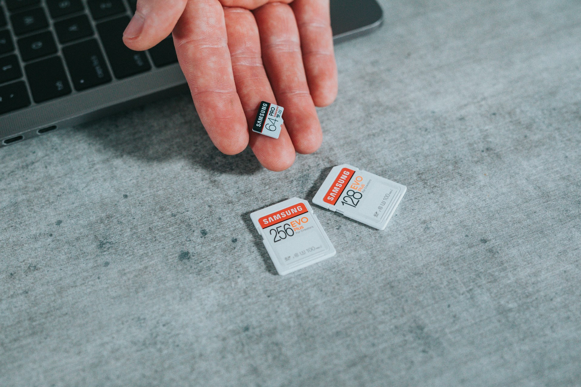
“Most people are familiar with NAND flash memory because it’s the kind that is in the memory cards for digital cameras and thumb drives. It is also used in computers and mobile phones. Making this type of memory denser still; so that more data can be packed into the same footprint, will be increasingly important as our data storage needs grow due to the use of artificial intelligence,”
stated Igor Kaganovich, a principal research physicist at PPPL.
“These processes use plasma as a source of high-energy ions,”
said Yuri Barsukov, a former PPPL researcher now working at Lam Research.
The investigation looked at phosphorus trifluoride that improves silicon dioxide etching. The plasma process received acceleration when phosphorus trifluoride was added because it specifically improved etching rates of oxide layers. Scientists noted the outcome of ammonium fluorosilicate when this substance appeared during silicon nitride etching procedures. The inhibitors in the reaction operated at a slower rate yet the addition of water diminished their capabilities which produced efficient etching outcomes.
“Cryo-etch with the hydrogen fluoride plasma showed a significant increase in the etching rate compared to previous cryo-etch processes, where you are using separate fluorine and hydrogen sources,”
said Thorsten Lill of Lam Research.
As the demand for higher-capacity digital storage grows, researchers are refining the way 3D NAND flash memory is manufactured.
This research investigation creates better production techniques for NAND flash memory and contributes knowledge that helps optimise plasma interaction for multiple semiconductor technologies. Through optimised control of silicon-based material reactions with etching agents researchers establish foundational knowledge to improve microelectronic development.

Hassan graduated with a Master’s degree in Chemical Engineering from the University of Chester (UK). He currently works as a design engineering consultant for one of the largest engineering firms in the world along with being an associate member of the Institute of Chemical Engineers (IChemE).