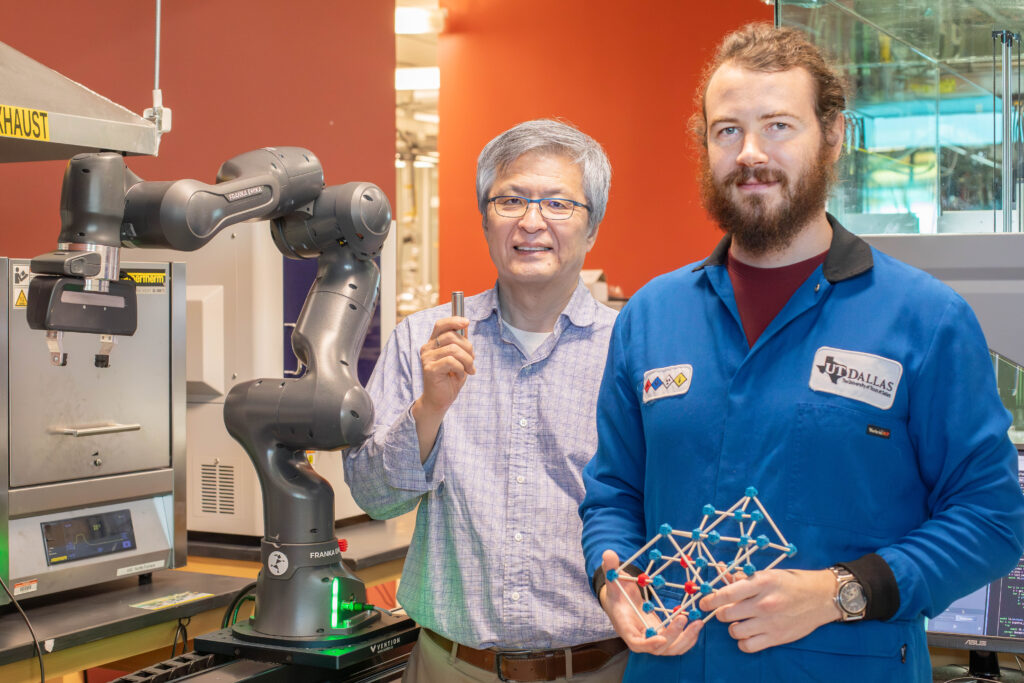
In a groundbreaking study, Dr. Jeremy Sloan and his team at the University of Warwick have advanced the synthesis of novel one-dimensional (1D) materials using carbon nanotube confinement. Their research opens new avenues for manipulating material properties at the atomic scale. You can view the published paper here:
Faulques, E., Ivanov, V. G., Cordier, S., Kashtiban, R. J., Molard, Y., Duvail, J.-L., Kalashnyk, N., & Sloan, J. (2025). Differential Packing of Cs 2 Mo 6 Br 14 Cluster-Based Halide in Variable Diameter Carbon Nanotubes with Elimination and Polymerization to 1D [Mo 2 Br 6 ] x Ising Model Structures by Steric Confinement. Journal of the American Chemical Society, 147(9), 7345–7359. https://doi.org/10.1021/jacs.4c14883
Further published papers provided by Jeremy Sloan are:
Halide perovskites in nanotubes
- https://advanced.onlinelibrary.wiley.com/doi/10.1002/adma.202208575
- https://pubs.acs.org/doi/10.1021/jacs.2c13711
Cluster ions
- https://doi.org/10.1007/s10876-014-0734-0
- https://doi.org/10.1007/s10904-014-0112-2
- https://doi.org/10.1016/j.jcis.2014.03.008
- https://doi.org/10.1002/adfm.201300417
Thermoelectric properties of crystals inside nanotubes
As part of our deeper dive into this emerging field, which we previously covered in a news report, we spoke with Dr. Sloan to explore the principles behind his work, the challenges of atomic-level synthesis, and the future potential of these confined materials in applications like quantum devices and thermoelectrics.
The following interview is presented unedited to preserve Dr. Sloan’s original responses and provide readers with an in-depth and authentic look at his research and its implications for materials science and quantum technologies.
Follow the Authors here:
- Eric Faulques | Linkedin
- Victor Ivanov | Linkedin
- Stephane Cordier
- Reza Kashtiban | Linkedin
- Yann Molard | Linkedin
- Jean Luc Duvail
- Nataliya Kalashnyk | Linkedin
- Jeremy Sloan | Linkedin
Acknowledgment from Dr. Jeremy Sloan: This work was supported by the French-Bulgarian PHC RILA project N° 38661ZF “EOPEN”. Some facilities used in the present research are part of the Distributed Research Infrastructure INFRAMAT, supported by the Bulgarian Ministry of Education and Science. V.G.I. would like to acknowledge financial support from the European Union-NextGenerationEU, through the National Recovery and Resilience Plan of the Republic of Bulgaria, Project No. BGRRP-2.004-0008-C01. J.S. and R.J.K. are indebted to the EPSRC (U.K.) for support under Grant No. EP/R019428/1. Electron microscopy at Warwick is supported by the University of Warwick’s Research Technology Platforms.
Could you explain the key principles behind the carbon nanotube confinement method and how it enables the synthesis of novel 1D materials?
The key principle in carbon nanotube confinement is primarily steric confinement which are normally non-bonding interactions between the host (i.e. the carbon nanotube) and the guest material (in this case the cluster anion or Cs2Mo6Br14.
The full confinement effect occurs once the internal diameter (ID) of the host nanotube approaches the outside diameter (OD) of the guest species. The ID of the nanotube is mostly provided by the diameter of the nanotubes but also the physical size of the nanotube carbon atoms, often referred to as the ‘van der Waals’ surface or Radii. (Note: the name van der Waals comes from the Dutch physicist Johannes Diderik van der Waals, 1837-1923).
However carbon nanotubes, as conjugated p-systems, can also interact chemically or with the guest with the wall carbons either absorbing positive charge from the guest or donating negative charge to the guest. This phenomena may contribute to some of the observed chemical rearrangements that we see although some of the primary effects are driven by steric confinement, in the first instance.
How does the structural confinement within nanotubes influence the electronic and quantum properties of the synthesised materials compared to their bulk counterparts?
This phenomena relates to type of material that is being encapsulated and how that material responds to encapsulation. We find for example that thermoelectric materials, like tin telluride, undergo an enhancement to the ‘Seebeck Coefficient’ which is a measure of the ability of a material to convert heat to electricity. Other semiconducting materials undergo a predicted expansion in their semiconducting bandgap as they become smaller and smaller.
In the case of the cluster compound Cs2Mo6Br14, this material is known for its photoluminescent light emitting characteristics but, as our paper shows, this material transforms chemically, due to the confinement effect, into the Ising-Like structure and inorganic polymer [Mo2Br6]x which consists of a chain of Mo2Br6 units.
(Notes from Press release provided by Matt Higgs, Media & Communications Officer (Sciences), Warwick); The Ising model (or Lenz–Ising model), named after the physicists Ernst Ising and Wilhelm Lenz, is a mathematical model of ferromagnetism in statistical mechanics. The model consists of discrete variables that represent magnetic dipole moments of atomic “spins” that can be in one of two states (+1 or −1). The spins are arranged in a graph, usually a lattice (where the local structure repeats periodically in all directions), allowing each spin to interact with its neighbours. Neighbouring spins that agree have a lower energy than those that disagree; the system tends to the lowest energy, but heat disturbs this tendency, thus creating the possibility of different structural phases. The model allows the identification of phase transitions as a simplified model of reality. The two-dimensional square-lattice Ising model is one of the simplest statistical models to show a phase transition.
What challenges did your team face in controlling the atomic arrangement and stability of these 1D materials inside nanotubes, and how were these challenges overcome ?
We synthesise the confined materials using one of three main synthetic protocols – introduction through the vapour phase (i.e. sublimation), introduction from a melt (this is controlled by capillary action) or introduction from solution (i.e., the species is first dissolved and then deposited inside carbon nanotubes from solution).
The obtained encapsulated materials are then imaged by aberration corrected electron microscopy to view the atomic structures of the encapsulated materials which are measured and then simulated using proposed models and through extended studies, we can solve the encapsulated crystal structures.
Computation can assist here in two important respects: (i) it can calculate the electronic properties of the encapsulated structures based on their solved crystal structures. This data can then be used to compute spectra (e.g. Raman or optical) which can be measured form the obtained materials; (ii) another approach (not this study) can be used to predict what structures can form. These results can then be compared against the experimentally obtained crystal structures.
How do the unique quantum properties of these confined materials contribute to advancements in quantum computing, and what specific applications do you foresee?
We are still at the relatively early stages of studies into the quantum behaviour of these materials but certainly experiments can be conducted in order to study the quantum properties of these materials.
One technique could be electron spin resonance (EPR) which can examine the spin properties of the encapsulated materials.
Two additional important aspects in terms of realising the applications of these materials are processing and purification (or cleaning). Processing can be in terms of refining the nanotubes. Normally these are supplied in the form of unsorted nanotubes of varying diameter which is initially important in terms of determining what type of crystal structure forms in what diameter nanotube – an issue we reviewed extensively in the JACS manuscript.
Processing will be necessary in future samples to produce composite materials which only one type of nanotube and one type of embedded crystal structure. Additionally, we want to use other types of processing to try to produce orientated bundles and thin films for possible device applications.
After nanotubes are filled with a particular material, some purification will be necessary to remove the excess filling material from outside of the nanotubes.
What characterisation techniques, particularly in electron microscopy, were crucial in confirming the formation and properties of these new materials?
Electron microscopy is used in several ways to confirm the crystal structures of the filling materials. Non exhaustively: (i) to analyse the crystal structures formed; (ii) to confirm the chemical identities of the elements in the embedded crystal structures e.g. by X-ray microanalysis, electron energy loss spectroscopy or by using the atomic thickness density to distinguish light and heavy elements; (iii) we also use microscopy to ascertain the filling ratio (i.e. number of filled vs. unfilled carbon nanotubes).
We also use various bulk methods to characterise the samples including XPS which adds information about the chemical oxidation state of the elements in the filled sample, EPR, used to analyse the spin states present, Raman spectroscopy to evaluate any electronic change in the carbon nanotubes post filling and, more recently, ultrafast Terrahertz spectroscopy which can analyse changes in the nanotube and embedded crystal conductivity. We are also using SQUID to analyse changes in magnetic behaviour of embedded magnetic materials.
How scalable is this method for producing 1D materials in quantities suitable for practical applications, and what are the next steps toward commercialisation or integration into quantum devices?
Current size scales are of the order of milligram to gram scale but some companies now are capable of produced kg or higher quantities of nanotubes.
For some (e.g. thin film) applications, milligram to gram scale is already enough but in future it may be necessary to produce these materials on a larger scale and that is also currently possible.
Looking ahead, what other material systems do you plan to explore using nanotube confinement, and are there collaborations underway to expand the applicability of this technique?
We have a particular focus now on investigating ferromagnetic or paramagnetic materials inside nanotubes although some groups are already looking at the detector capability of (for example) halide perovskites embedded in carbon nanotubes.
We would like to extend our studies into thermoelectric materials and try to investigate materials which are semiconducting in nanotubes which are themselves semiconducting.
Given the results of the current work, we in particular would like to investigate Ising like structures and see if we can develop and make use of their spin characteristics and develop them further as useful materials with regards to their use in information storage and so on.

Hassan graduated with a Master’s degree in Chemical Engineering from the University of Chester (UK). He currently works as a design engineering consultant for one of the largest engineering firms in the world along with being an associate member of the Institute of Chemical Engineers (IChemE).