Semiconductors are everywhere. They power the smartphones in our pockets, the laptops on our desks, and the cars we drive. They enable the high-speed processing in our computers, the data transmission in our wireless networks, and even the advanced imaging capabilities of medical equipment. Yet, for all of their ubiquity, semiconductors remain largely invisible to most people. What exactly is a semiconductor? And how did it become so essential to modern society?
In this article, we will explore the fascinating journey of semiconductor technology—from its early roots in 19th-century science, through the groundbreaking invention of the transistor in 1947, to the cutting-edge materials that promise to shape the future of electronics. We’ll also take a look under the hood to understand how semiconductors work, the concept of the band gap, and how doping techniques revolutionized the field. By the end, you’ll have a deeper appreciation for the tiny devices that make our modern, connected world possible.
The History of Semiconductors
The story of semiconductors traces back to the early 19th century with the work of scientists like Michael Faraday, who studied the electrical properties of materials and laid the groundwork for future advancements in semiconductor physics. However, the true tipping point came in 1947, when John Bardeen, Walter Brattain, and William Shockley at Bell Labs invented the transistor. This tiny device replaced bulky vacuum tubes, making it possible to build smaller, more efficient electronic devices. Fast forward to today, and semiconductors form the backbone of our modern world—from computing and telecommunications to artificial intelligence and beyond.
What Is a Semiconductor?
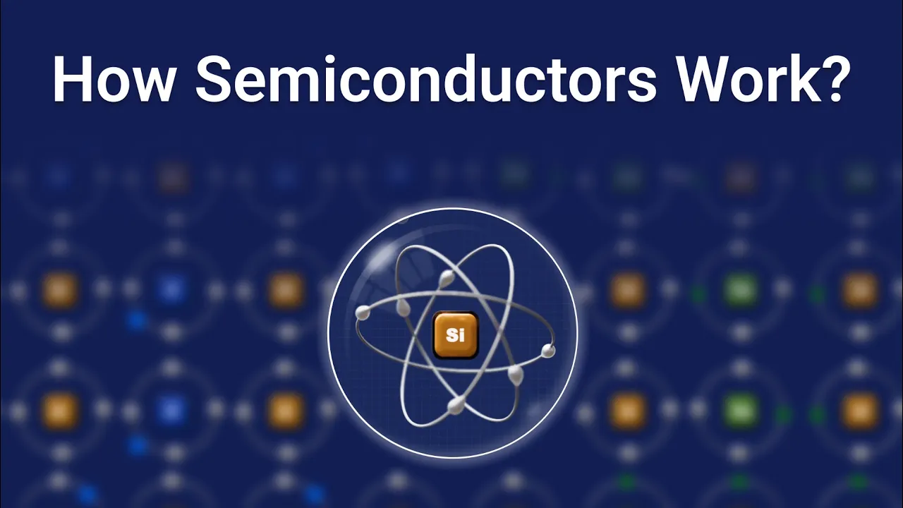
At its core, a semiconductor is a material with electrical conductivity that lies between that of a perfect conductor (like copper) and an insulator (like rubber). This unique property allows semiconductors to act as controllable gateways for electrical current.
Band Gap Energy
Unlike conductors, where electrons move freely, semiconductors have an energy gap—known as the band gap—between the valence band (where electrons are bound to atoms) and the conduction band (where electrons are free to move). For instance, silicon has a band gap of about 1.1 eV, making it ideal for microelectronics, while gallium arsenide (GaAs), with a band gap of 1.43 eV, is preferred for high-speed and optoelectronic applications such as laser diodes and solar cells.
In simpler terms, the band gap is small enough that electrons can be “kicked” from the valence band to the conduction band under the right conditions—heat, light, or an external voltage—enabling controlled electrical conductivity.
Here’s a quick breakdown of materials based on their band gap energy:
- Conductors (e.g., copper, silver): Essentially no band gap; electrons move freely.
- Semiconductors (e.g., silicon, germanium): Small band gap; electrons can move with a bit of external energy (heat or light).
- Insulators (e.g., rubber, glass): Large band gap; very few electrons can move.
Band Gap Energy Equation
Eg = h/λ
- Eg: is the band gap energy
- h: is Planck’s constant (6.626 x 10^-34 J s)
- c: is the speed of light (3 x 10^8 m/s)
- λ: is the wavelength of the absorption edge
Controlling Conductivity through Doping
One of the most fascinating aspects of semiconductors is that their conductivity can be modified through a process called doping—introducing small amounts of impurity atoms into the semiconductor crystal. These impurities either donate free electrons or create “holes” where electrons can jump, thus altering the material’s electrical properties.
Types of Doped Semiconductors
- N-Type Semiconductors
- Doped with elements like phosphorus or arsenic, which have extra electrons to offer.
- These surplus electrons freely move, creating a negatively charged environment.
- P-Type Semiconductors
- Doped with elements like boron or gallium, which have fewer electrons.
- “Holes” or vacancies are created, effectively acting like positively charged carriers.
When you combine n-type and p-type semiconductors, you form a PN junction—the fundamental building block of many electronic components, including diodes, transistors, and solar cells.
Different Types of Semiconductors
Though silicon is the undisputed king of modern electronics, various semiconductor materials cater to different applications:
- Silicon (Si): The most widely used semiconductor in everything from computers to smartphones.
- Germanium (Ge): Historically significant but less common today due to cost and material properties.
- Gallium Arsenide (GaAs): Ideal for high-speed and optoelectronic devices, such as radar and satellite communications.
- Silicon Carbide (SiC) & Gallium Nitride (GaN): Gaining traction in power electronics and electric vehicles for their efficiency and ruggedness.
- Organic Semiconductors: Emerging area for flexible electronics, wearables, and advanced displays.
Researchers around the globe are pushing the boundaries of semiconductor technology with quantum semiconductors, nanoelectronics, and biocompatible materials. These innovations promise faster computing, enhanced medical devices, and a host of breakthroughs we can only begin to imagine. Yet, hurdles like material stability, fabrication costs, and manufacturing scalability remain. Overcoming these challenges will pave the way for the next revolution in electronics.

Hassan graduated with a Master’s degree in Chemical Engineering from the University of Chester (UK). He currently works as a design engineering consultant for one of the largest engineering firms in the world along with being an associate member of the Institute of Chemical Engineers (IChemE).